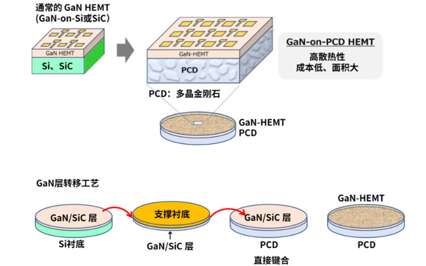
Si (silicon) and SiC (silicon carbide) are commonly used as substrates for GaN-HEMTs, but diamond has a thermal conductivity approximately 12 times higher than Si and 4–6 times higher than SiC, thereby reducing thermal resistance by 1/4 and 1/2, respectively.
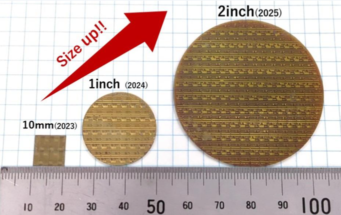
To date, it has been difficult to directly bond GaN layers without solder or adhesive materials due to the large grain size and high surface roughness (5–6 nm) of polycrystalline diamond. However, by combining diamond substrate polishing technology—which reduces surface roughness to half that of conventional methods—with a technique for transferring GaN layers from Si substrates to polycrystalline diamond, we have successfully bonded GaN layers directly to 2-inch polycrystalline diamond.
This demonstrates the feasibility of GaN structures on polycrystalline diamond and the uniformity of their thermal dissipation characteristics.